CMOS Infrared Photodetector
Synopsis
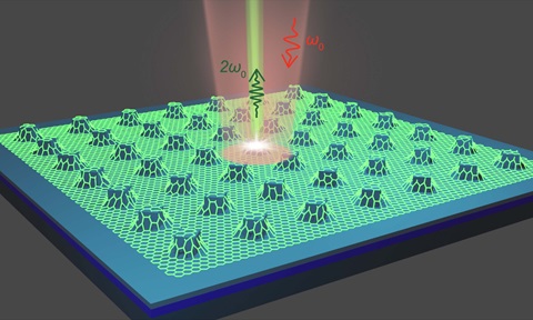
This technology presents a complementary metal-oxide semiconductor (CMOS)-compatible approach for fabricating germanium (Ge) micro- and nano-structures, leading to potential applications in infrared (IR) photodetectors. This device exhibits antireflection properties with reflectance as low as five per cent in the IR range of 2-5 µm, making it an effective IR absorber.
Opportunity
Anisotropic wet etching using acid to form inverted pyramid structures has been widely used in the CMOS flow of silicon (Si) industries for applications in MEMS and optoelectronics. However, such CMOS-compatible anisotropic wet etching techniques are still scarce for Ge industries. This technology presents the formation of microscale Ge inverted pyramid and v-groove structures by wet etching acid solution catalysed by CMOS-compatible metals. Both titanium nitride (TiN) and titanium/nickel (Ti/Ni) catalysts have been proven feasible, and their long-term durability in etchant has also been verified. The dimensions of Ge structures are determined by the patterned catalyst, allowing for easy tuning of the desired sizes of the Ge inverted structures. The Ge microscale textures show outstanding anti-reflective performance in the IR range.
The targeted users of this technique are Ge-based MEMS and optoelectronic device manufactures who require CMOS-compatible fabrication processes and potential antireflective performance of Ge substrates. This is similar to current Si-based CMOS manufacturers using Si inverted pyramidal structures with wet acid.
Technology
This novel wet etching technique fabricates inverted pyramid and v-groove structures of Ge using a noble metal-free, metal-assisted chemical etching process. The etched Ge textures exhibit outstanding antireflection performance in the IR range. The etching process is catalysed by CMOS-compatible metals, specifically TiN or Ti/Ni.
Applications & Advantages
Main application areas include Ge MEMS and optoelectronic devices, such as IR photodetectors.
Advantages:
- Exhibits reflectance as low as 5% in the IR range of 2-5 µm.
- The dimensions of Ge structures can be easily tuned based on the patterned catalyst.


.tmb-listing.jpg?Culture=en&sfvrsn=3b74ec1c_1)


.tmb-listing.jpg?Culture=en&sfvrsn=414f0d90_1)


