Integrated Photonics for Stable Ion-Trap Qubit for Quantum Computing, Multi-Channel Optical Transceiver and LiDAR Applications
Synopsis
This novel electro-optical module for trapped ion enables large-scale fabrication of compact quantum chips using CMOS technology. Integrating silicon photonics and ion traps, it enhances quantum computing efficiency with over 50% footprint reduction, on-chip integration of wavelength filters and photon detectors. Suitable for quantum sensing, computing, LiDAR, and multi-channel optical transceivers, the technology owner seeks partners for ion traps, photon detection, LiDAR and optical transceivers.
Opportunity
In certain types of quantum computing, trapped ions are used as qubits for performing computing operations. However, the challenge to maintain stability of the trapped ion for as long as possible remains.
This technology is a novel design of photonics device/circuits arrangement that facilitates the optical addressing of trapped ions. This can be applied in quantum technologies such as quantum clock and quantum computing. In the case of quantum computing, its fundamental concept involves usage of trapped ions as quantum bits for computational purposes.
The electro-optical module in this design is feasible in wafer-scale fabrication using conventional CMOS technology. By further integration with state-of-the-art 3D-packaged ion traps, it yields opportunities in large-scale fabrication of compacted quantum computing chips, like the fabrication of CMOS chips for conventional computing purposes.
The coupling of laser light into the chip has always been a significant technical challenge in silicon photonics. At the same time, packaging optical fibre onto silicon photonics chips conventionally has a high form-factor. The integration of wavelength-filtering ring resonator enables coupling of multiple wavelengths using only one inlet.
The technology owner is looking for partners in quantum sensing and computing application where ion traps and selected photons detection is required. In addition, they are interested in collaborations involving the application of multi-wavelength LiDAR and multi-channel optical transceivers.
Technology
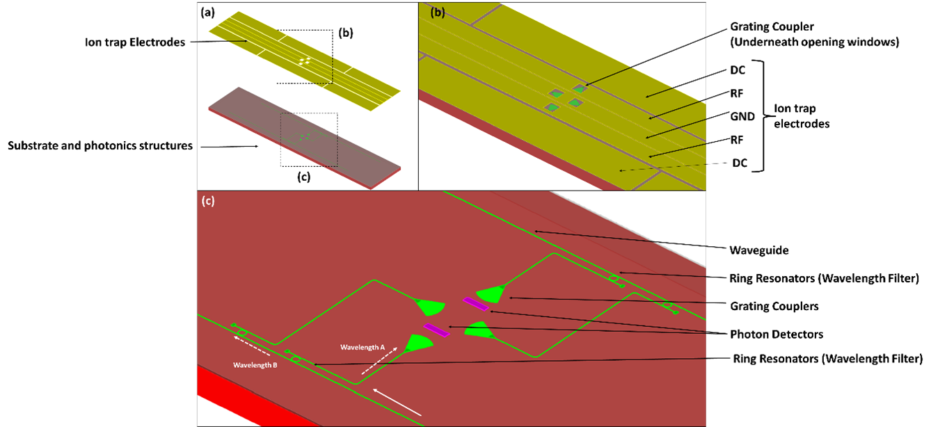
The technology involves electro-optical integration of both passive and active silicon photonics components and the planar electrode ion trap. Two major parts of the technology are photon detection by inter-electrode detector placement, and wavelength filtering with multi-layer ring resonator.
Photon detection is mainly used in ion trap applications. The photodetector is conveniently placed beneath the gaps between ion trap electrodes. Thus, no additional openings are needed for the detection of photons emitted from the trapped ion. This increases efficiency while reducing the form factor.
Wavelength filtering can be generally used in multi-wavelength coupling. The customised design of ring resonator is able to channel laser source with mixed wavelengths into the silicon chip, and split two separated wavelengths into designated waveguides.
The demonstration, in the case for ion-trap for quantum computing, has been realised for wavelengths at 1092 and 1033 nm laser beams which are specific for such a use case.

Figure 1: Ion-trap for quantum computing and LIDAR applications.
Applications & Advantages
Applications:
- Ion trap quantum computing – compact design (>50% form factor reduction), reduces number of fibre coupling, minimal disruption in ion-trapping operation
- LiDAR – enables multi-wavelength scanning on two separated emission sources, reduces number of fibre coupling
- Multi-channel optical transceivers – enables co-fabrication of transceivers with different optical bands on the same chip.
Advantages:
- Increased quantum computing efficiency by optimising laser wavelength filtering and photon detection from ion-trap electrodes, hence minimising operational disruption.
- Miniaturisation achieved by integrating on-chip wavelength filters and photon detectors, reducing footprint by over 50% and eliminating the need for extensive fibre coupling.


.tmb-listing.jpg?Culture=en&sfvrsn=57e7d9a3_1)
.tmb-listing.jpg?Culture=en&sfvrsn=40b426f_1)


